Q-Switch Driver
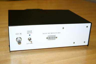
The Q-Switch driver for an old Yag laser died. A replacement was >$1000 so we built our own for <$300 (picture and schematic below). The specs were >= 20W into a 50 ohm load at 68MHz. The rep rate had to be adjustable between 100Hz and 100KHz and have a TTL output to synchronize the output with other equipment.
RF Amp
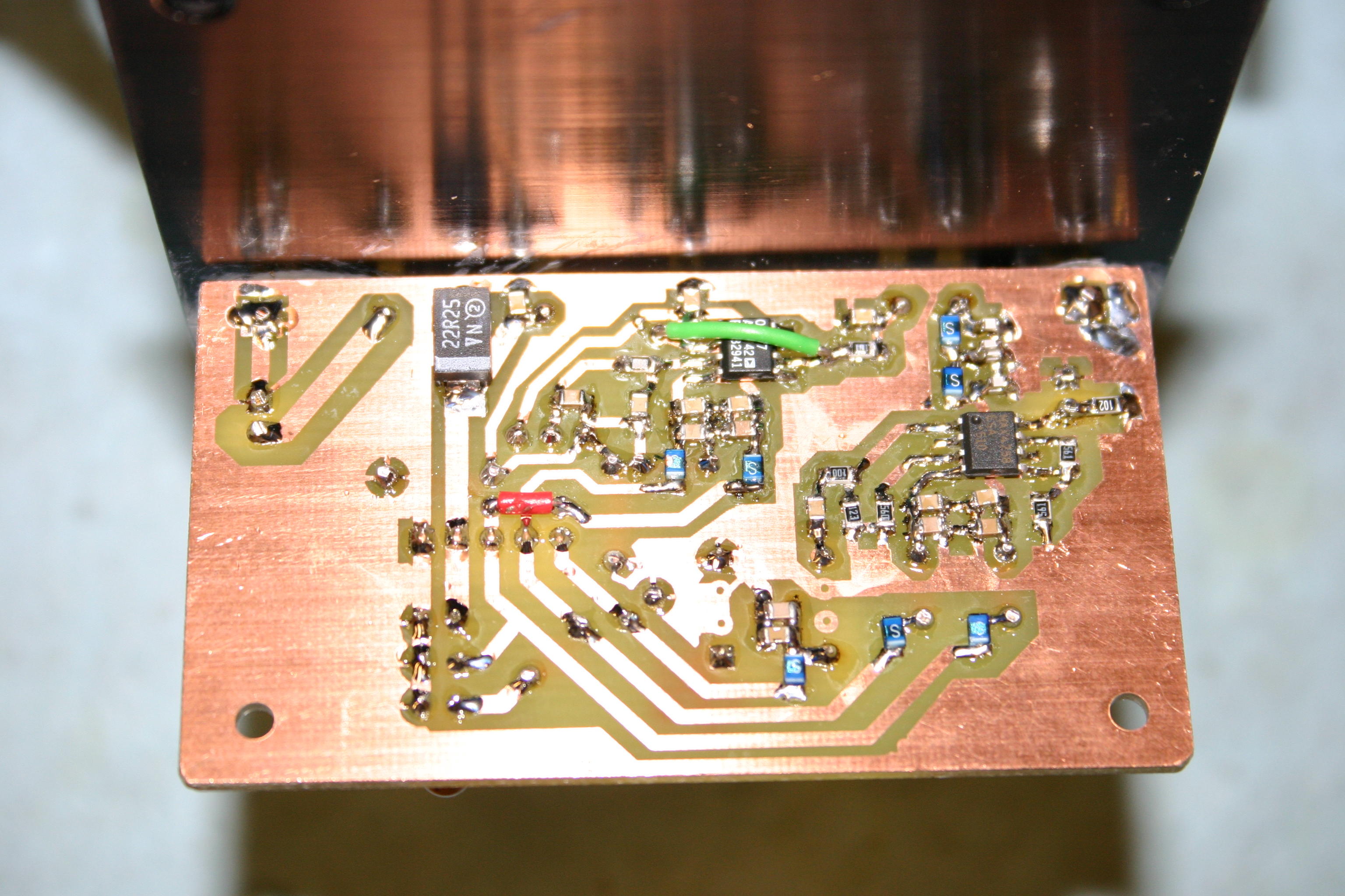
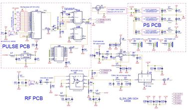
I had never made a RF amplifier before so for me that would be the tricky part. I started by ordering a 3.3V CMOS oscillator, CPPC4-LT5RP ($8.14), from www.digikey.com and having them program it for 68.000MHz. The square wave oscillator worked well but couldn't drive a 50 ohm load. I AC coupled the oscillator to a MAX4258 video driver/multiplexer. The AC coupling centered the oscillator at GND and the driver can drive a 50 ohm load. The multiplexer will later be used to quickly turn off the oscillator for about 6us (to q-switch the laser).
If I block all frequencies above the fundamental I can turn a square wave into a sine wave. An article on DDS IC's in Circuit Cellar pointed me to http://tonnesoftware.com/svcfilter.html. The filter software was easy to use and free. I was able to make a 5th order low-pass to block everything above 72Mhz. The 68MHz fundamental will pass but all the harmonics will be attenuated (Ex: The third harmonic, 204MHz, is attenuated by 50db).
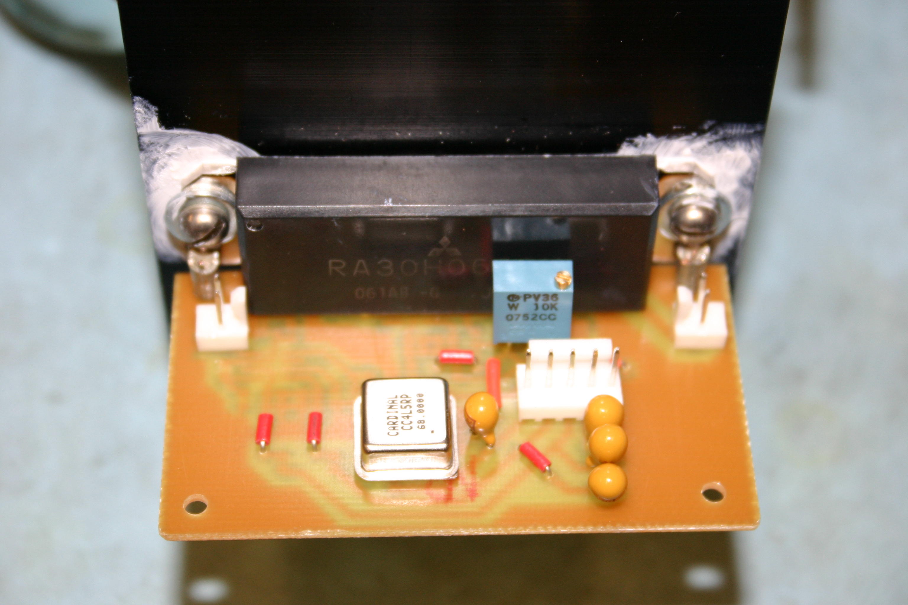
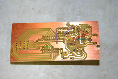
Now I have a 68MHz sine wave that's about 3Vpp (13dbm). Note: I need 20W (43dbm). We searched around and found the RA30H0608 from www.rfparts.com ($73). Its specs are 68-88MHz, 30W output, 12V power supply, and it has a gate pin to modulate the output (i.e. control the gain). I used a trim pot to set a DC voltage, buffered it with an op-amp configured as a voltage follower, and sent it to the gate pin on the amplifier to control the gain. Note: Turning the RF off via the gate pin was slow (about 10us) so I used the mux on the video driver IC to turn the RF on and off (about 200ns). I purchased a SWR/Watt-meter (MFJ-872 from www.mfjenterprises.com for $100) and adjusted the trim pot to get 20W from the amp. A TTL input to the MAX4258 is used to modulate the RF. This takes care of the RF section. Pictures of the RF board are shown below.


Control Logic
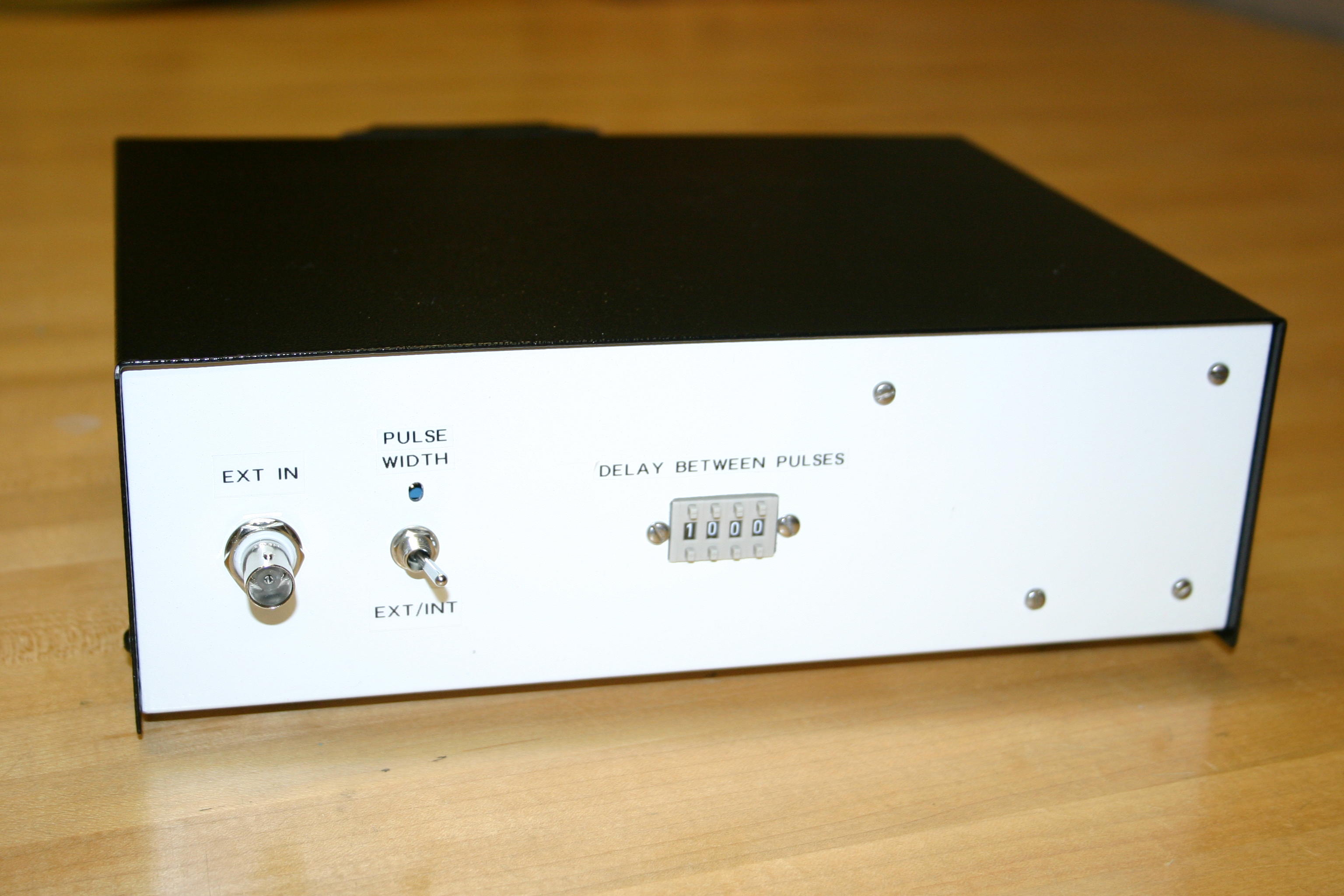
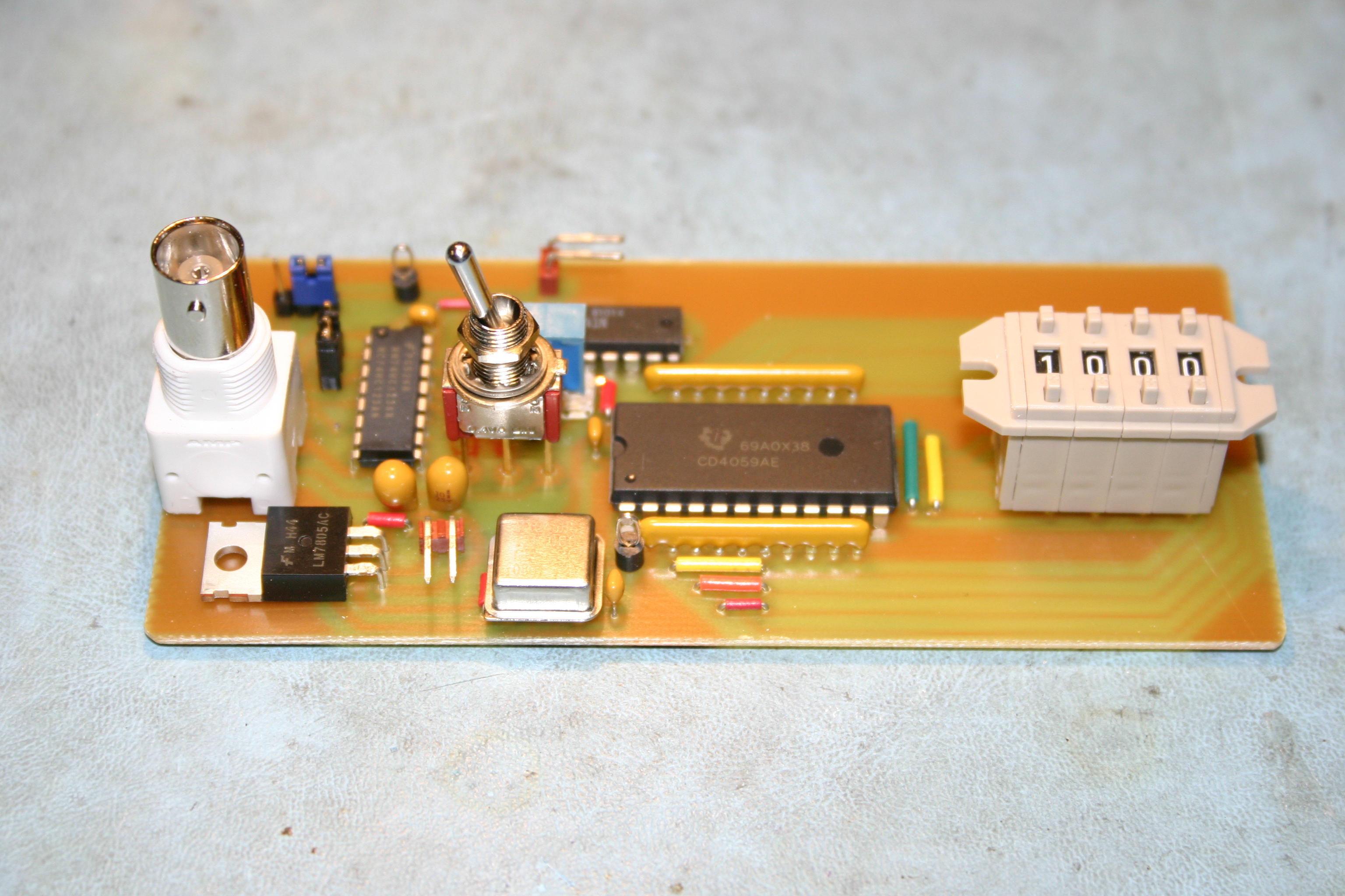
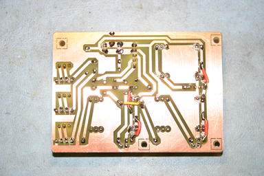
The rep-rate of the laser had to be adjustable (100Hz-100KHz using the internal circuitry) and have the option of being controlled by an external TTL input. I decided to keep it simple. Instead of using a DDS chip or a microcontroller to allow for frequency input I used programmable counter to let the user input the time between laser pulses. The user enters the time into the CD4059 counter using BCD thumbwheel switches. A 1MHz oscillator provides the time base (1us per # set on the thumbwheel). The counter output (or an external TTL input) drives a 74HC123 one-shot to provide a pulse that's about 6us long (adjustable with a trim pot). The output of the one-shot is used to trigger the MAX4258 multiplexer on the RF board and also drive a 74LS241 buffer to provide a TTL output for other equipment. Pictures of the logic circuit board are shown below.

Power Supply
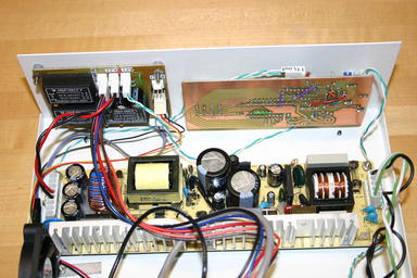
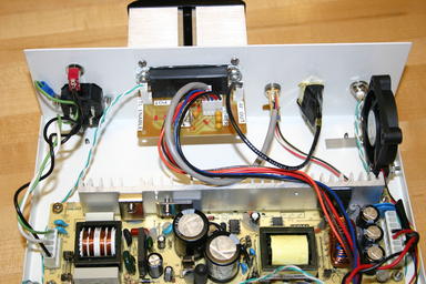
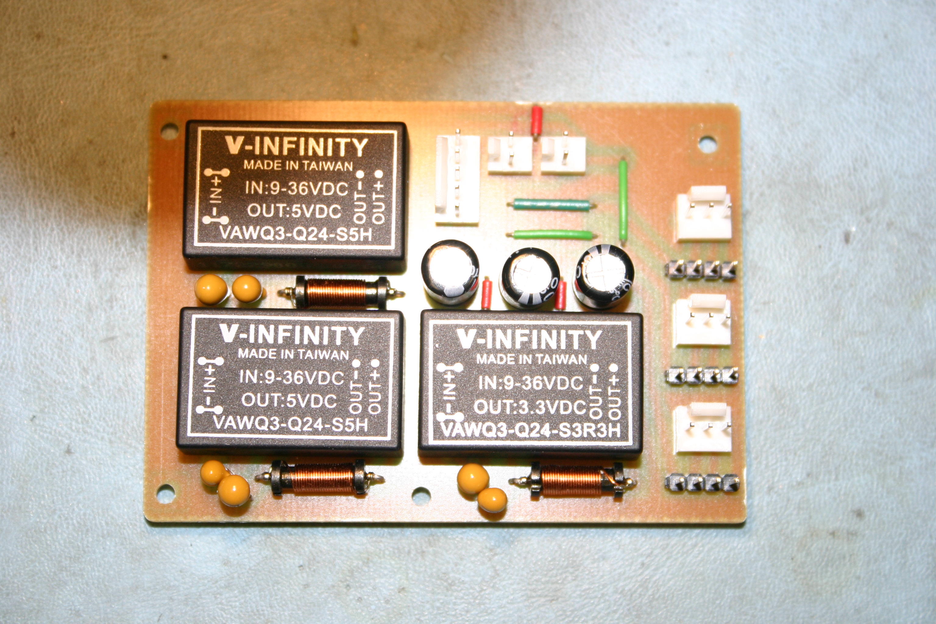
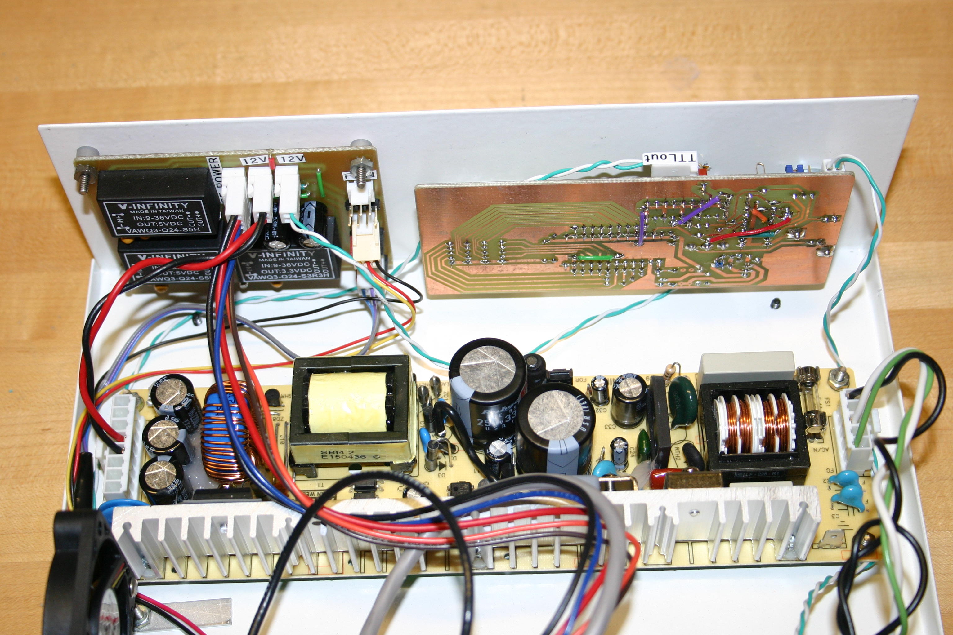
The RF amp needs 12V@4-5A to produce 20W (about 40% efficient). I bought a 100W, 12V switching supply from www.jameco.com for $56. The RF board also needed +5V, -5V, & +3.3V. I used DC/DC converters on a separate power supply board to convert the 12V supply to the needed voltages. I also added headers to run 12V fans (one to blow air across the RF amp heatsink and one to circulate air through the enclosure to cool the switching supply). Pictures of the power supply pcb are shown below.

Decoupling and Filtering
All IC's are decoupled from the power supply with bypass caps. The RF board is small and uses SMT parts with caps very close to the parts. In addition, most of the RF parts have small inductors in series with the power supply to help filter out high frequencies. The trim pot that controls the gain on the RF amp is low pass filtered at the trim pot and again at the gate pin to remove any noise.
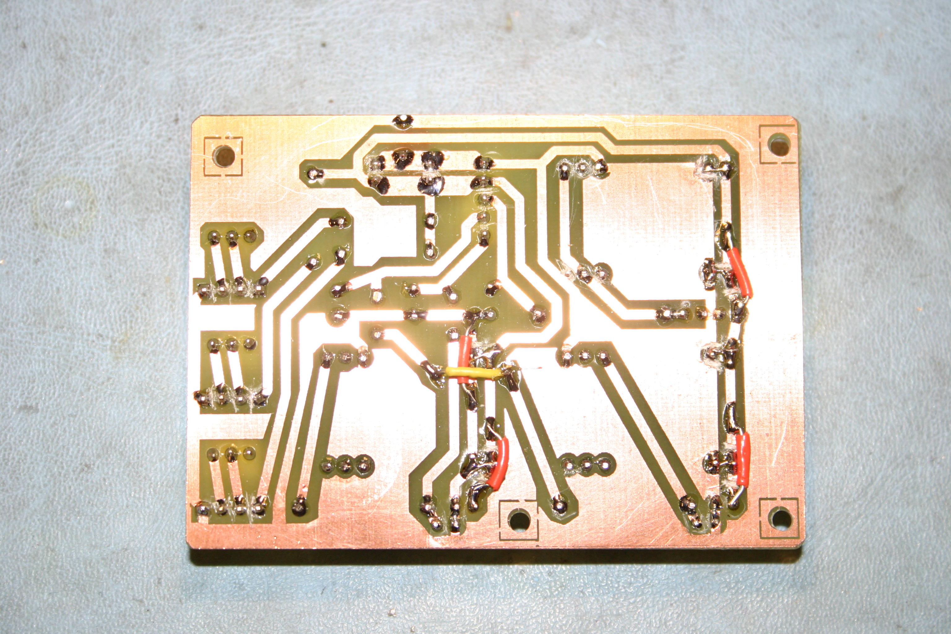
Printed Circuit Boards
We have a setup to make single sided PC boards so I mad the boards in house (easier for prototyping). Ideally the RF board would be smaller with multiple layers (including a ground plane) but with careful layout, I was able to get by with a single sided PCB. Having a maximum frequency of 68MHz and keeping the traces as short as possible helped. Links to postscript files of the board layout are below. Note: When making the PCB you want the print side of the transparency to be against the PCB. Therefore the RF board (SMT board) was made using the bottom view (mirrored) file and the control and power supply boards (through hole boards) use the top view file.
Silkscreen (Top View)
Silkscreen mirrored (Bottom View)
Pic showing all the traces (Top View)
Pic showing all the traces mirrored (Bottom View)
Solder (Top View)
Solder mirrored (Bottom View)
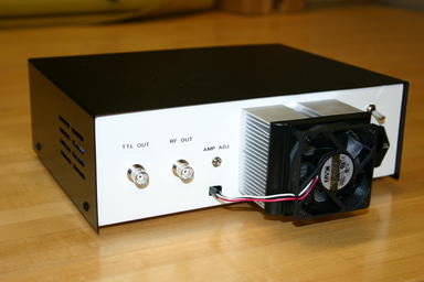
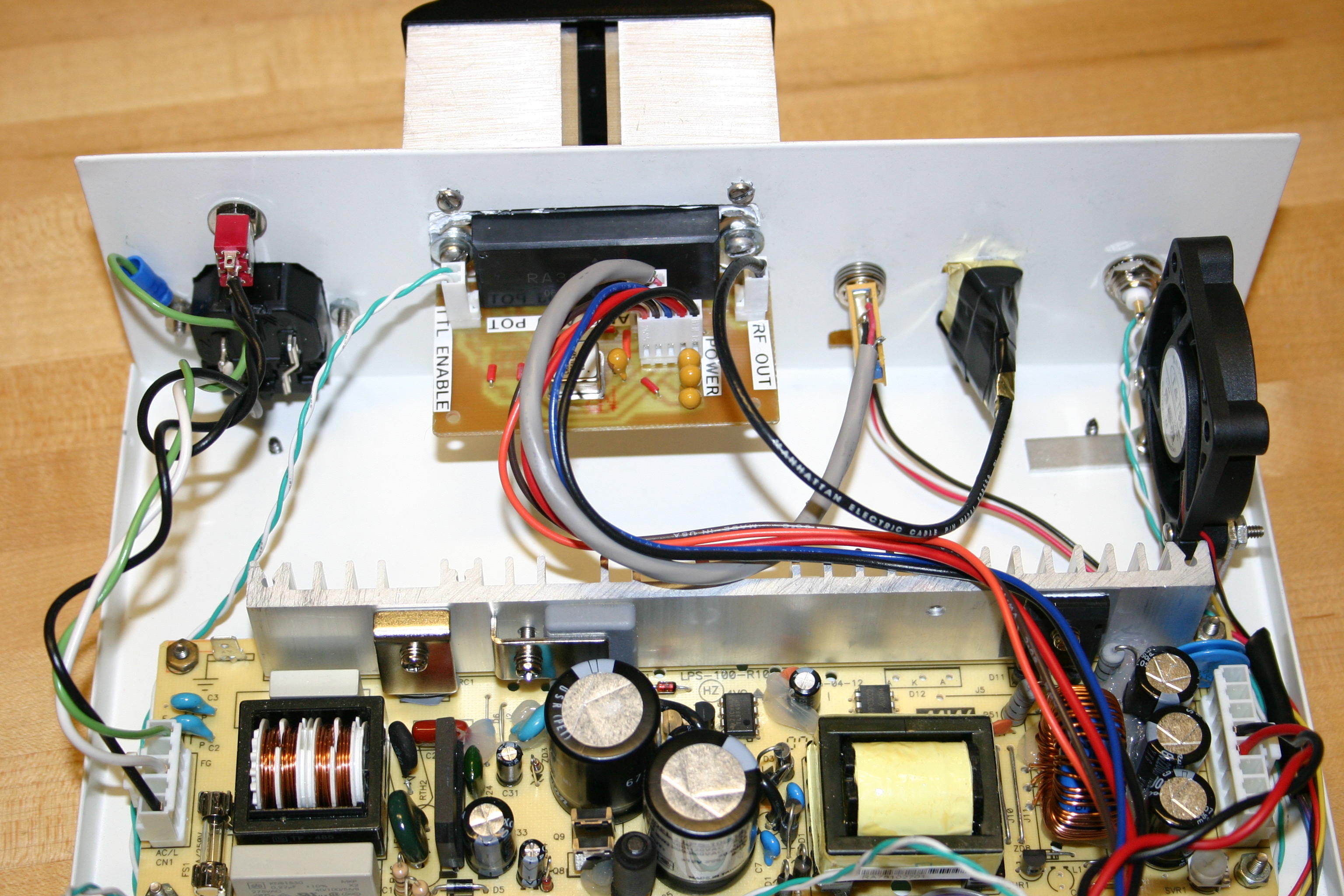
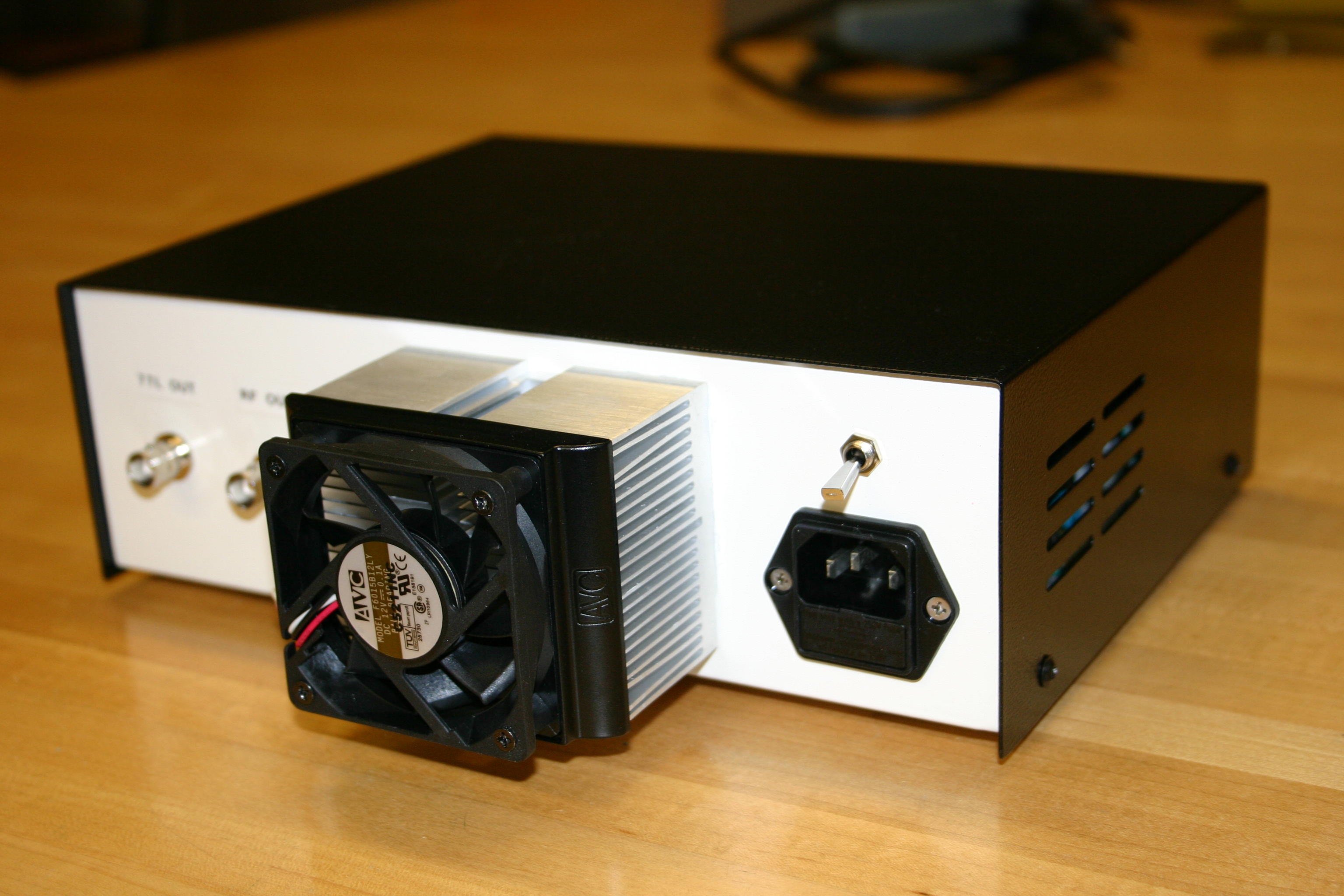
Pictures of the inside and a rear view of the box