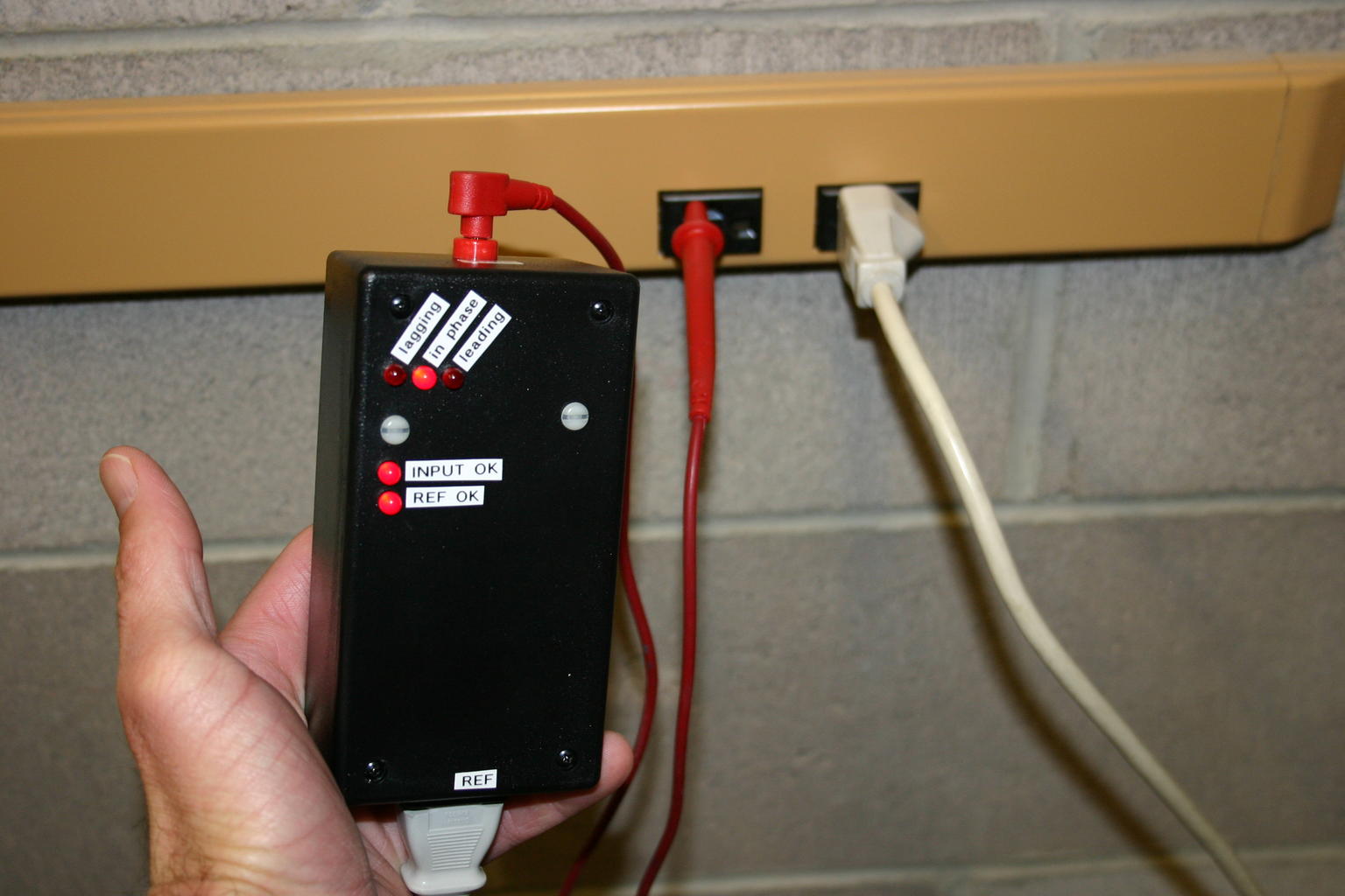
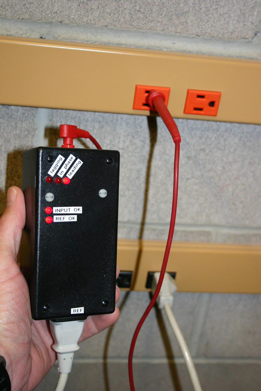
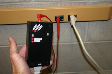
Phase Detector (i.e. which phase is this outlet on?)
 Problem:
We wanted to balance the load in our computer rooms across all three phases (less chance of blowing the main circuit breaker). We didn't know which outlets were on which phases. At first I used a scope set to trigger on line and went around poking a wire in each outlet to see if it was leading, lagging, or in phase (referenced to the outlet the scope was plugged into). Dragging a scope around to every outlet got annoying quickly.
Solution:
I decided to build a circuit to take the place of the scope (one of three LED's would light to let me know which phase the outlet is on. The circuit works by squaring up the two signals to be compared (input and reference) and comparing when the rising edges occur. If the rising edges come in at the same time they're in phase, if the input rising edge comes in before the reference it's leading, and if the input rising edge comes in after the reference it's lagging.
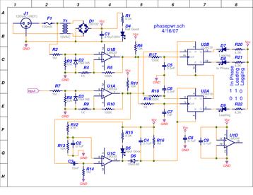

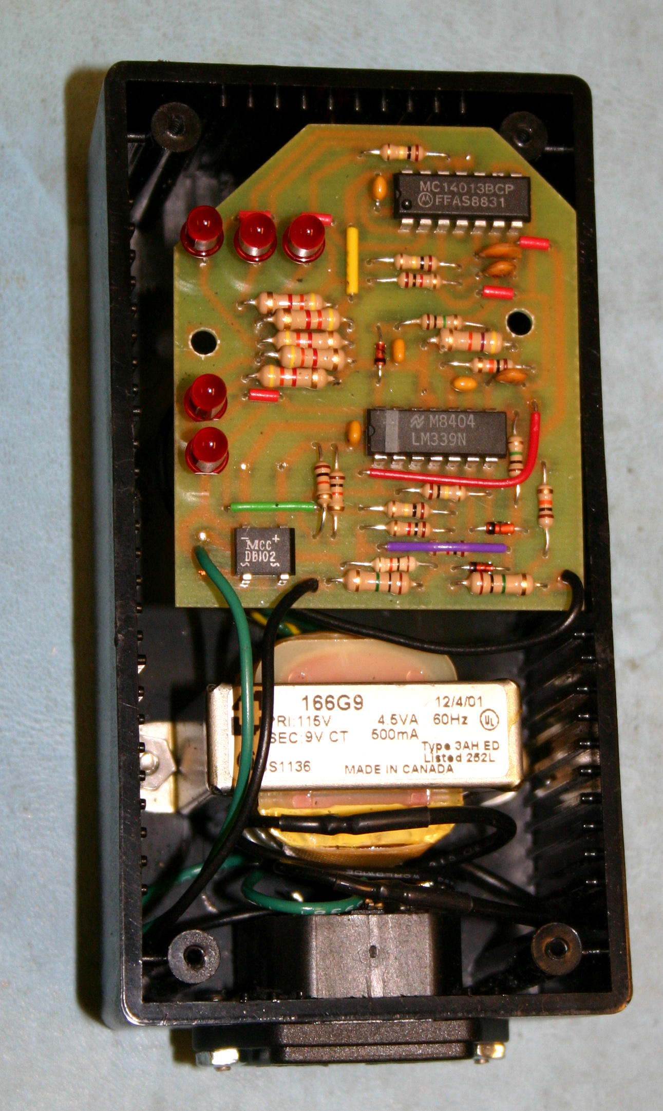
A voltage divider is used to drop the voltage down to a safe level (R2 & R3) and a comparator is used to square it up around the zero point. Diodes (D2) were used to make sure the input doesn't go negative since I'm using a single power supply (GND to 9V). R4 & R5 provide a little hysteresis so the output doesn't temporarily oscillate when switching states. R6 is a pullup (open collector outputs on the LM339).
Both flip-flops are clocked in on the rising edge of the reference but R17 & C5 delay the clock signal for U2B about 200us where as R19 & C17 don't noticeably delay the clock on U2A. Note: R19 & C17 are there for noise control (shorting high frequency noise to ground). Without the RC filter the flip-flop would trigger multiple times (noisy power supply maybe). Similarly R18 & C6 delay the input to U2A but the input to U2B isn't delayed.
When the input is in phase with the reference both rising edges occur at the same time. U2B has the clock delayed and the input arrives without delay so its output goes high. U2A has the clock arrive without delay and the input is delayed so its output goes low. Therefore when the input and reference are in phase Q_U2B = 1, Q_U2A = 0. When the input is lagging the reference (i.e. 120 degrees back @ 60hz = 5.5ms) both D inputs are low when clocked so both Q outputs are low. When the input is leading the reference both D inputs are high when clocked so both Q outputs are high. The above description would be true if the Set & Reset pins on the flip-flop were low (inactive) all the time. But to decode the binary output (leading = 11, in-phase = 10, lagging = 00) so only one LED comes on at a time the Set & Reset pins were used to disable the flip-flops at certain times. Note: when Set & Reset are both high both Q and Q_NOT are high and the LED's are off.
C3 & R14 AC couple the input to U1C. U1C compares the input to a reference voltage (a volt or two above ground). Since C3 & R14 only pass AC signals the output of U1C will be high when there is no input present and will oscillate when there is a valid input (i.e. the input probe is shoved in a hot plug). D6, C4, & R16 rectify the output oscillation and hold the Set and Reset pins on U2A low when there is a valid input and high when the input isn't valid (which keeps D9 from lighting without a valid input). The output of U2A also holds the Set & Reset pins low when D9 is lit insuring that only one of the three LED's is on at a time. The other two LED's light to show valid inputs. The circuit is powered through the reference input so whenever there is power the REF LED is on. Whenever the output of U1C oscillates (meaning there is a large AC voltage at the input) the INPUT LED will light which allows the other LED's to come on.
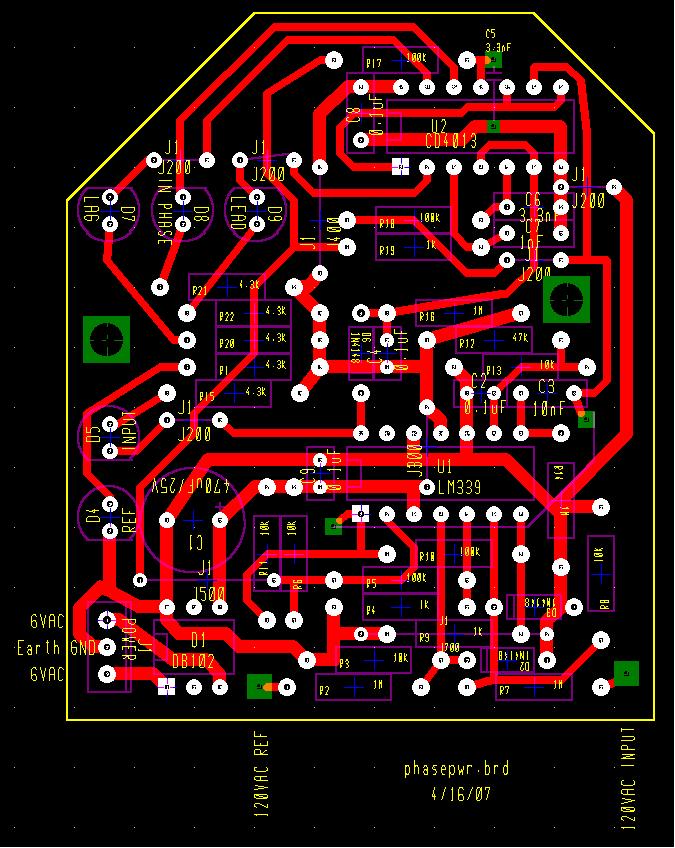
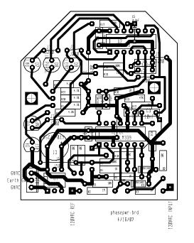
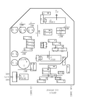
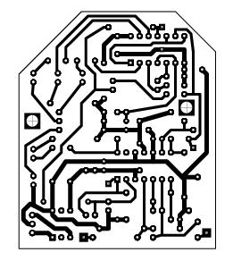
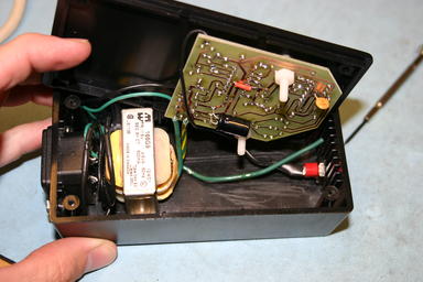
The board layout is below. The PDF files should print 1:1 for making the PCB.