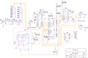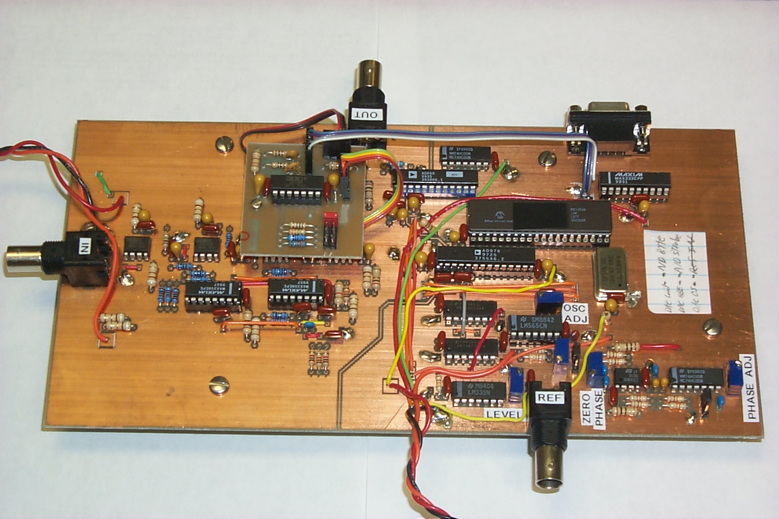
The purpose of a Lockin Amplifier is to amplify signals at the reference frequency and reject signals at other frequencies. The left side of the board is the analog side. There is a buffer, two programmable gain stages and an output buffer. The output buffer originally drove the input to a 16 bit A/D converter but we later added an analog integrator (the small board on top) before the A/D. The amplified signal is integrated for 1/2 the reference period and then digitized. Sequential values are added and subtracted removing all signals not at the reference frequency. The microcontroller (uP) adds a fixed number of cycles and spits the result out a serial port to a PC at up to 115K baud. The uP also sends the output to a 16 bit buffered D/A converter, thus an analog output is also available (once programmed the lockin can be used without a PC). All variables are programmable from the PC (gain, reference frequency, # of cycles to sum, etc.). The IC's in the lower right comprise a phase-lock-loop to lock to an external reference. This never quite worked as planned so we locked the beam chopper to the reference generated on the board.
This was a proof of concept device. We originally thought we needed four lockin amplifiers to do an experiment. It would be quite expensive to buy for lockins with GPIB capability to record the data. Although the lockin worked as planned we found other analog methods to reduce noise such that lockin amplifiers wern't needed.